BENDIX BENDIX 7129 Manual de usuario Pagina 3

  • Descarga
  • Añadir a mis manuales
  • Imprimir
  • Pagina
    / 20
  • Tabla de contenidos
  • MARCADORES
  • Valorado. / 5. Basado en revisión del cliente
Vista de pagina 2
ADV7129
–3–
REV. 0
TIMING SPECIFICATIONS
Parameter Conditions Min Typ Max Units
CLOCK CONTROL & PIXEL PORT
4
LOADIN Clocking Rate, f
LCLK
10 45 MHz
LOADIN Cycle Time, t
1
16.67 ns
LOADIN Low Time, t
2
6.67 ns
LOADIN High Time, t
3
6.67 ns
LOADIN to LOADOUT Delay, t
4
5ns
Pixel Setup Time, t
5
10 ns
Pixel Hold Time, t
6
42 ns
MPU PORT
R/
W, C0, C1 Setup Time, t
7
10 2.5 ns
R/
W, C0, C1 Hold Time, t
8
10 0.5 ns
CE Low Time, t
9
25 ns
CE High Time, t
10
25 ns
CE Asserted to Data-Bus Driven, t
11
25 ns
CE Asserted to Data-Bus Valid, t
12
20 ns
CE Negated to Data-Bus Invalid, t
13
1ns
CE Negated to Data-Bus Three Stated, t
14
15 ns
Write Data (D7–D0) Setup Time, t
15
10 ns
Write Data (D7–D0) Hold Time, t
16
10 ns
ANALOG OUTPUTS
5
Analog Output Delay, t
17
@ 360 MHz 5 ns
Analog Output Rise/Fall Time, t
18
0.8 ns
Analog Output Transition Time, t
19
25 ns
RGB Analog Output Skew, t
SK
1.5 ns
Pipeline Delay, t
PD
19 PCLKs
PLL PERFORMANCE
6
Jitter (1σ) (LOADIN = 45 MHz) 55 ps rms
NOTES
1
TTL inputs values are 0 V to 3 V with input rise/fall times 3 ns, measured between the 10% and 90% points. Timing reference points at 50% for inputs and out-
puts. Analog output load 10 pF. Databus (D7–D0) loaded as shown in Figure 1. Digital output load for SENSE 30 pF.
2
±5% for all versions.
3
Temperature range (T
MIN
to T
MAX
), 0°C to +70°C.
4
Pixel Port consists of the following inputs: Pixel Inputs: RED [A-H], BLUE [A-H], GREEN [A-H].
5
Output Delay is measured from the 50% rising edge of LOADIN to the 50% point of full-scale transition on the A pixel. t
17
includes the analog delay due to DACs
and internal gate transitions plus the pipeline stages delay. The output delay for pixels B-H will be the output delay to the A pixel (t
17
) plus the appropriate number
of clock cycles. Output rise/fall time is measured between the 10% and 90% points of full-scale transition. Settling time is measured from the 50% point of full-scale
transition to the output remaining within 1%. (Settling Time does not include clock and data feedthrough.)
6
Jitter is measured by triggering on the output clock, delayed by 15 µs and then measuring the time period from the trigger edge to the next edge of the output clock
after the delay. This measurement is repeated multiple times and the rms value is determined.
Specifications subject to change without notice.
(V
AA
2
= +5 V, V
REF
= +1.235 V, R
RSET
, R
GSET,
R
BSET
= 280 V, R
L
= 25 V for IOG, IOR, IOB, C
L
= 10 pF.
All specifications T
MIN
to T
MAX
3
unless otherwise noted.)
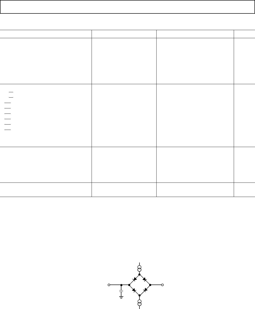
TO OUTPUT PIN +2.1V
100pF
I
SINK
I
SOURCE
Figure 1. LOADIN vs. Pixel Input Data
Vista de pagina 2
1 2 3 4 5 6 7 8 ... 19 20

Comentarios a estos manuales

Sin comentarios